What can we get From LEED?
LEED is the principal technique for the determination of surface structures. It may be used in one of two ways:
1. Qualitatively: where the diffraction pattern is recorded and analysis of the spot positions yields info on the size, symmetry and rotational alignment of the adsorbate until cell with respect to the substrate unit cell.
2. Quantitatively: where the intensities of the various diffracted beams are recorded as a function of the incident electron beam energy to generate so-called I-V curves which, by comparison with theoretical curves, may provide accurate info on atomic positions.
Principles and Diffraction Patterns
By the principles of wave-particle duality, the beam of electrons may be qually regarded as a succession of electron waves incident normally on the sample. These waves are diffracted by regions with high localised electron density (the atoms).
The wavelength of the electron is given be the de Broglie relation:
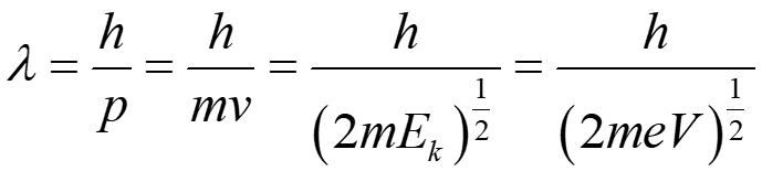
where λ is the wavelength and p is momentum.
The rangle of wavelengths of electrons employed in LEED experiments is seen to be comparable with atomic spacings, which is necessary condition for diffraction effects associate with atomic structure to be ovserved.
Consider, first, a 1D chain of atoms (with atomic spacing Å) with the electron beam incident at right angles to the chain (this is the simplest possible model for the scattering of electrons by the atoms in the topmost layer of a solid; in which case the diagram below would be representing the solid in cross-section with the electron beam incident normal to the surface form the vacuum above. The electrons in the range of 20 to 200 eV can penetrate the sample for about 10 Å without loosing energy.
Consider, again, the backscattering of a wavefront from 2 adjacent atoms at a well-difined angle, \(θ\), to the surface normal then it is clear that there is a “path difference” (d) is the distance the radiaton has to travel from the scattering centres to a distant detector (which is effectively at indinity) – this path difference is best illustrated by considering 2 “ray paths” such as the right-hand pair of green traces in the above diagram.
The size of this path difference is asinθ and this must be equal to an integral number of wavelengths for constructive interference to occur when the scattered beams eventually meet and interfere at the detector i.e.

For two isolated scattering centres the diffracted intensity varies slowly between zero (complete destructive interference; d = ((n+1/2)λ) and its maximum value (complete destructive interference; d = nλ)-with a large periodic array of scatterers, but, the diffracted intrensity is only significant when the “Brag condition” is satified exactly. The diagram below shows tupical intensity profile for this case.
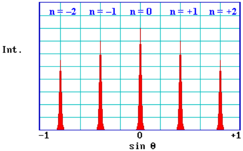
A number of points worth noting from this simple 1-D model
- the pattern is symmetric about θ = 0 (or sinθ = 0)
- sinθ is proportional to 1/V1/2 (since λ is proportional to 1/V1/2)
- sinθ is inversely proportional to the lattice parameter, a
the aforementioned points are infact much more general-all surface diffracton patterns show a symmetry reflecting that od surfce strcutre, are centrally symmetric, and of ascale showing an inverse relationship to both the squre root of the electron energy and the size of the surface unit cell.
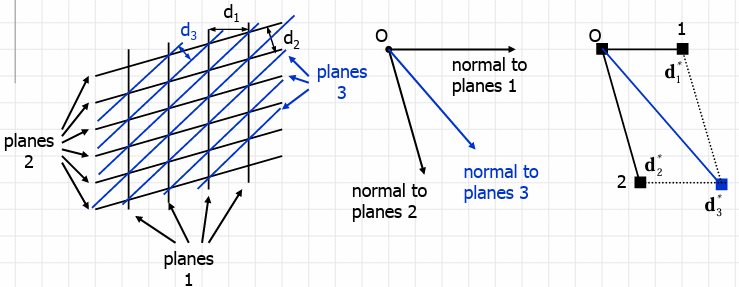
In LEED, the diffracted beams impact on a fluoresecnt screen and form a pattern of light spots, which is a to-scale version of the reciprocal lattice of the unit cell. The reciprocal lattice is a set of imaginary points, where the direction of a vector from one point to another point is equal to another point
Experimental Equipments
Back-Display LEED-AUGER optics and Power Supply
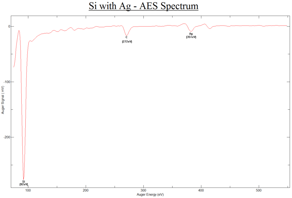
A commericial spectrometer have been assembled in the Preparation Charmber as shown in Figure 1 (http://www.ocivm.com/index.html) [If other excellent Co. also selling it, plz let me know]. Spectrometer is used to study of strcuture of the first few atomic layers of cyrstalline surfaces based on LEED effect and performs indentification of elemental components on the surface via spectroscopy of Auger electrons.
Operating Instruction
1.Ensuring preparation pressure (Pp) < 2×10⁻⁹ Torr.
2.Assembly line: ULVAC LEED-AES Controller terminal
LEED mode selected; Manipulator V2–Control Panel 1 LEED V2; Manipulatro C—ULVAC LEED/AES controller LEED C; monitor Is with tester (~20 uA).
3. Insert sample holder in Manipulator; the position of Manipulator is neighbour to (10, 15, 15).
4. Controller power is On
5. Filaments trun on to right, 6.9. IE should not exceed 2 mA.
6. Turn on “Lower”, Acceleration Voltage of electron gun is 90-115 eV.
7. Turn on “Screen” to kV.
8. Emission turn, It change to best, stop.
9. When It change to lagest, regulate Emission, Accelaration Voltage and Contrast, focus, (x, y, z).
10. When you can see LEED patterns and sports is clearly, regulate Emission, Accelaration Voltage and Contrast, focus, (x, y, z).
Note:
1. At RT, the filament can be exposed to atomspheric pressure repeatedly without impairing its emission characteristic.
Analysis Software
To my best konw, there are some software for free employed to anlyze LEED parterns. One of them is the this Enhance your LEED Analysis – LEEDLab and LEEDCal (fritz-sojka-gbr.de). Another one is ImageJ (ImageJ Wiki).
LEED and AES Data Library
Unit cell content: coordinates of all atoms; types of atoms; site occupancy; individual displacement parameters. They can be represented by symmetry operators.
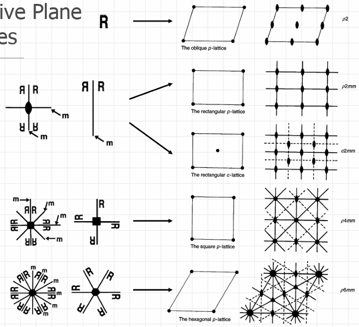
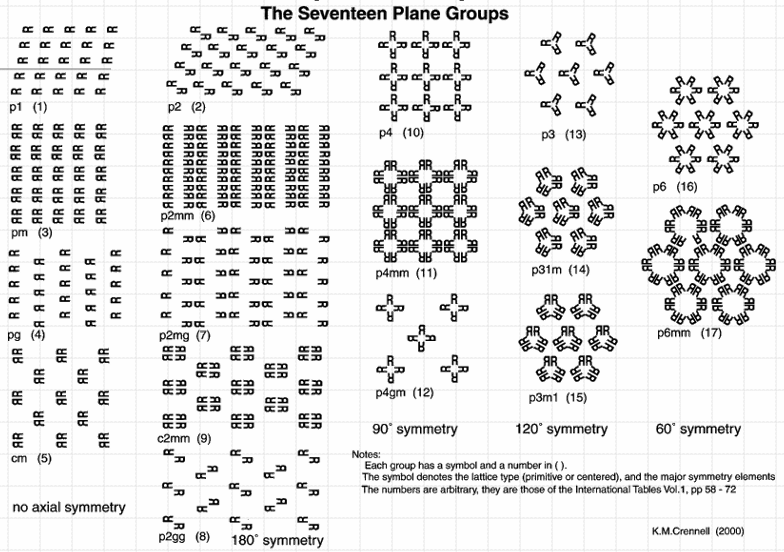
Symmetry is a property of a crystal which is used to describe repetitions of a pattern within that crystal.

2D symmetry elements (10 two-dimensional cyrstallographic or plane point groups): One-folf axis (no symmetry); Vertical mirror line; vertical and horizontal mirror lines; two-fold rotation axis; three-fold rotation axis; three-fold axis + vertical mirror line; four-fold axis; four-fold axis + mirror lines; six-fold axis; six-fold axis + mirror lines.
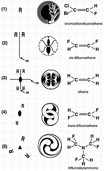
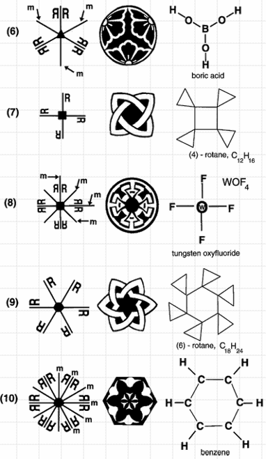
For 2D Bravais lattice, there are four kinds of crystal family and 5 Bravais lattice.

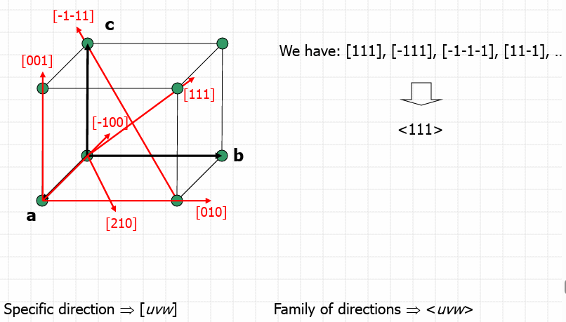
Indexing Lattice Directions
Direction must pass through the origin;
Coordinates of point P (in fractions of a, b and c) are 1, 1/2, 1-[212]
For point Q coordinates are 1/2, 1/4, 1/2-[212]
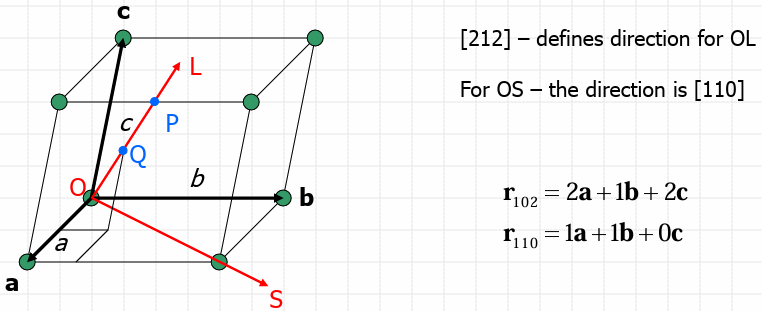
Specific direction-[uvw] Family of directions-[uvw]
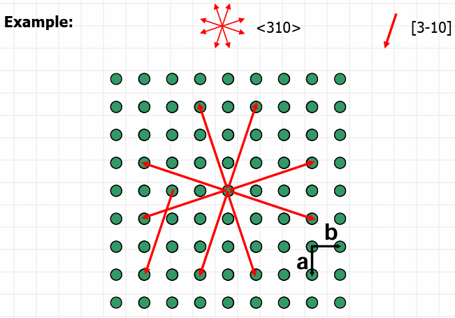
Directions related by symmetry are called directions of a form.
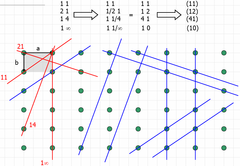
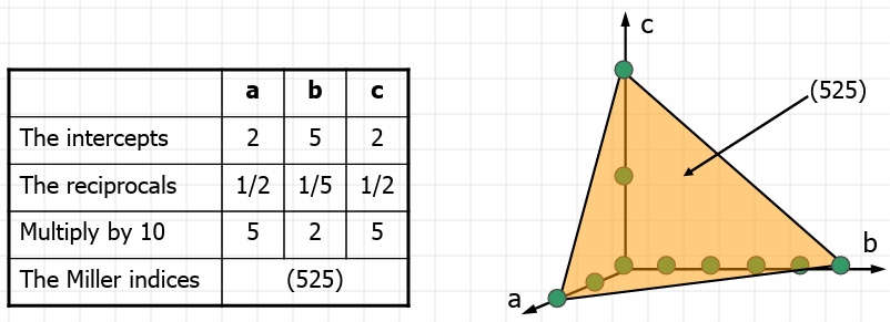
Definition of the Miller Indices
Let’s draw a plane at 2xa, 5xb, 2xc.
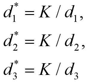
The Reciprocal Lattice
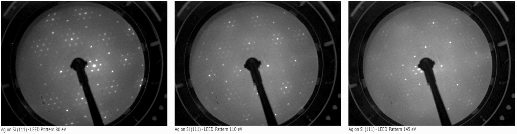
Ag/Si(111)-Silver on Silicon
| Size: 10x10x0.5 mm | Film Growth Method: Ag powder diffusion |
| Structure: Diamond Cubic | Melting T: 1414 °C |
| Lattice Constant: a = 5.43 A | Debye T (at 27 °C): 370 °C; Surface Debye T unpublished |
| Type/Dopant: N type/Undoped | UHV Treatment: Annealing at 270 °C (estimated T of sample)for 30 sec |